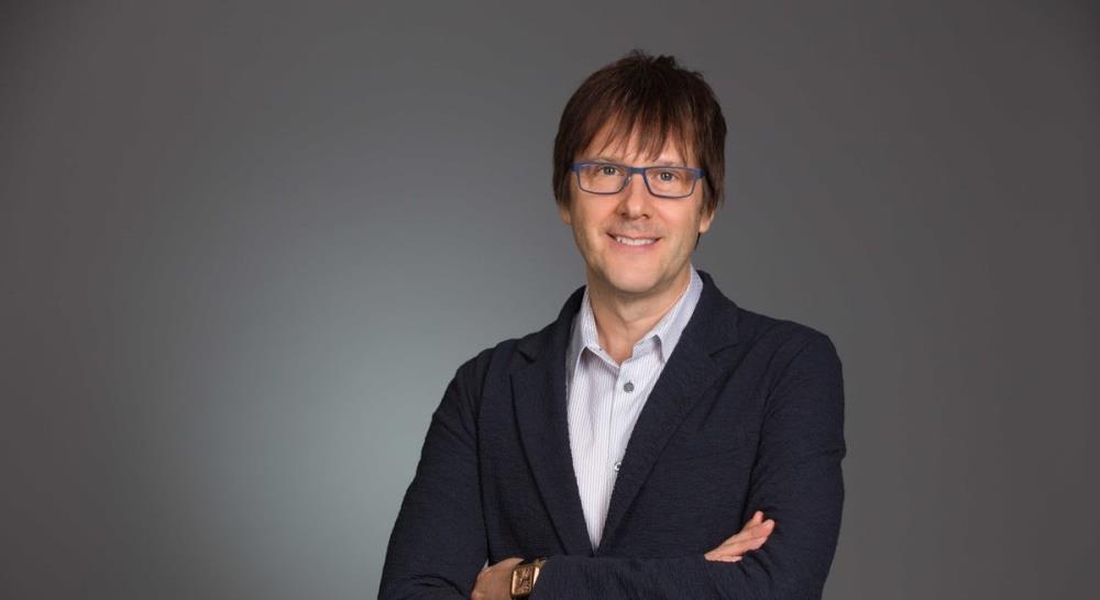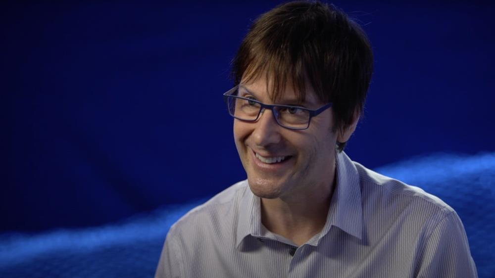
The PS4′s loving dad (or at least one of its fathers) Mark Cerny did a lot of thinking on the console’s architecture even before the first piece of circuitry was printed, so he's the best one to explain how the much touted 8 gigabytes of unified GDRR5 RAM coupled with the bus work, and why that solution was implemented.

PlayStation legend Mark Cerny discusses PS5, the challenges of making consoles, and his 42-year games industry career
Well... they used to design their own chips. Emotion Engine, Cell, RSX... when they switched to using X86 based chips is now more akin to low-mid cost PCs than before. It may not look like a PC but it pretty much is one. I'd bet it could do productivity stuff just fine if they allowed it to.
Yah, hence the majority of the PS5’s hardware investment going towards an SSD instead of a GPU.
There are countless custom pc gaming rigs out there, and I bet none of them took an SSD-centric approach to their design, like the ps5 did.
I can see where he’s coming from re ps5 not just being a box with parts like a pc. They must also spend an awful lot on r & d just to design the thing so it has aesthetic appeal and typical Japanese with some sort of Philosopy behind the design. Would also think other factors around the custom airflow and the like would cost a lot given that it’s not a standard box shape

Mark Cerny talks to Digital Foundry about how Dolby Atmos support made its way to PlayStation 5.
Cerny points out the advantage that DF keeps referring to as a disadvantage. Developers don't need to do anything special to have overhead sounds mapped to height speakers. It's all built in and processed lag free on existing and future PS5 games. This is obviously a superior approach imo as it works with virtually any speaker configuration.
The truth is that Atmos is superior. Plain and simple. The devil prefer it over what sony is providing. It's the standard for games, movies and music.
Ah yes Mark, becuase less channels on a watered down feature is something to geek out about. You do realize you are getting atmos light right? Not for audiophiles. Totally designed for craptastic sound systems. It's all about tagging that name for a selling point.

Mark Cerny is a true veteran of the games industry. His name might be familiar to modern gamers due to the fact that he's worked as lead architect on several of Sony's consoles – and has even had input into some of the company's major software releases, such as Knack, The Last Guardian, Marvel's Spider-Man and Death Stranding – but his career stretches back to the very early years of the games industry.
Lol, love this image...
https://images.timeextensio...
Look at the balls on Cerny! He really does though. One of the greatest minds in the industry and knows how to get things done!
Is this available in video format? It's a damn long interview to read.. but I will, if no video
i love his breakdowns of the consoles, he explains things very well with that soothing voice ha
Why doesnt n4g just makes one article telling everything that mark cerny explain instead having so many articles on mark cerny explained this and that..
No offense n4g
Mark is spreading the second coming of the king of console. The book of revelation of gaming shall be fulfill this holiday 2013
I watched the whole youtube presentation posted by the official playstation channel, it was technical at some points but I was engaged for the whole 47 mins and I learned a lot even about previous playstation consoles. I was amazed at how involved Cerny was with playstation since day 1 in 1994 but only found out about him at the feb reveal for ps4
Cerny is very, very wise.
not in technical terms... just looking at that picture from the article comparing architectures..
the one on the left allows developers to acces the 176GB per seconds from the start
while the one on the right would only allow them to use 88GB per second at first
they would only unleash the other 1000GB when the small EDram chip or whatever is mastered right?
and that would take a few years.. im i right?